logo
Datasheet4U.com - 74LVC2G74
logo

74LVC2G74 Datasheet, flip-flop, NXP Semiconductors

74LVC2G74 Datasheet, flip-flop, NXP Semiconductors

74LVC2G74

datasheet Download (Size : 153.62KB)

74LVC2G74 Datasheet
74LVC2G74

datasheet Download (Size : 153.62KB)

74LVC2G74 Datasheet

74LVC2G74 Features and benefits

74LVC2G74 Features and benefits

I I I I Wide supply voltage range from 1.65 V to 5.5 V 5 V tolerant inputs for interfacing with 5 V logic High noise immunity Complies with JEDEC standard: N JESD8-7 (1.6.

74LVC2G74 Application

74LVC2G74 Application

using IOFF. The IOFF circuitry disables the output, preventing damaging backflow current through the device when it is po.

74LVC2G74 Description

74LVC2G74 Description

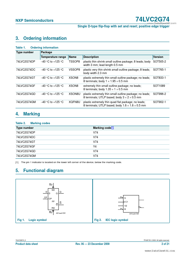
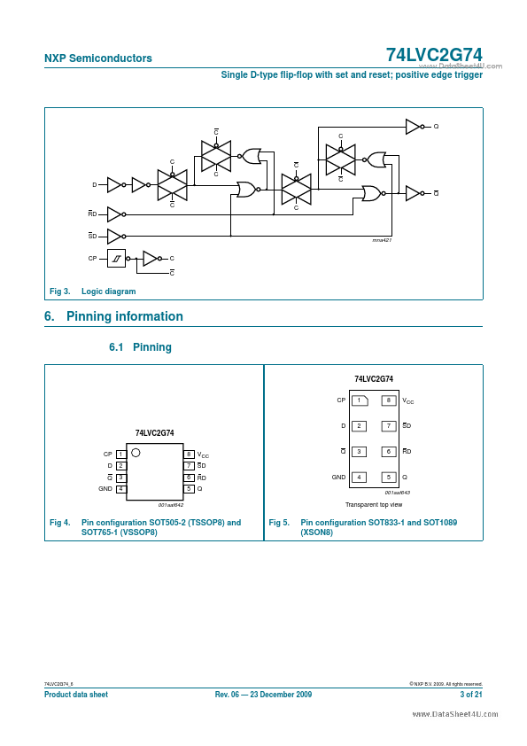
The 74LVC2G74 is a single positive-edge triggered D-type flip-flop with individual data (D) inputs, clock (CP) inputs, set (SD) and reset (RD) inputs, and complementary Q and Q outputs. This device is fully specified for partial power-down applications .

Image gallery

74LVC2G74 Page 1 74LVC2G74 Page 2 74LVC2G74 Page 3

TAGS

74LVC2G74
Single
D-type
flip-flop
NXP Semiconductors

Manufacturer


NXP (https://www.nxp.com/) Semiconductors

Related datasheet

74LVC2G74-Q100

74LVC2G00

74LVC2G00-Q100

74LVC2G02

74LVC2G02-Q100

74LVC2G04

74LVC2G04-Q100

74LVC2G06

74LVC2G06-Q100

74LVC2G07

74LVC2G07-Q100

74LVC2G08

74LVC2G08-Q100

Since 2006. D4U Semicon.   |   Datasheet4U.com   |   Contact Us   |   Privacy Policy   |   Purchase of parts